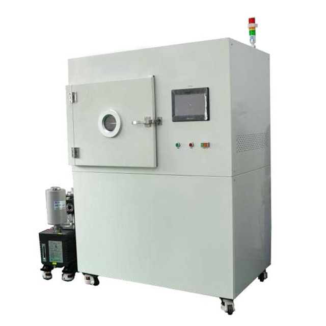
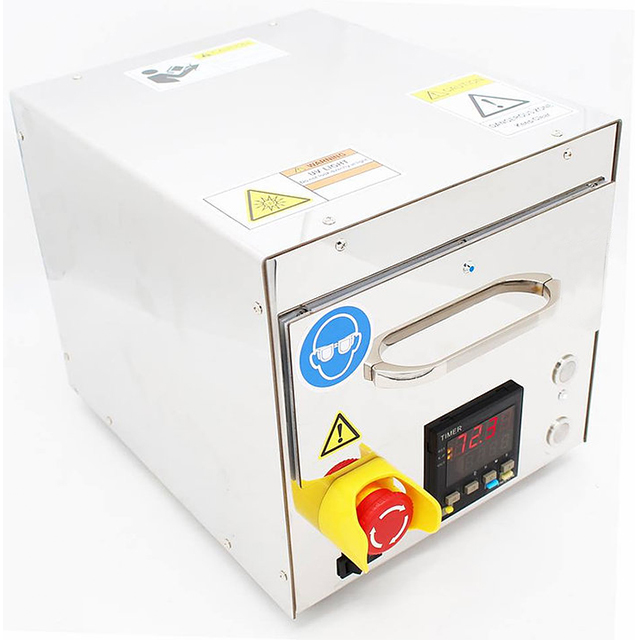
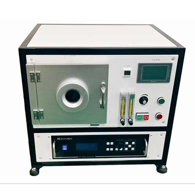
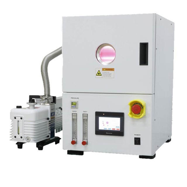
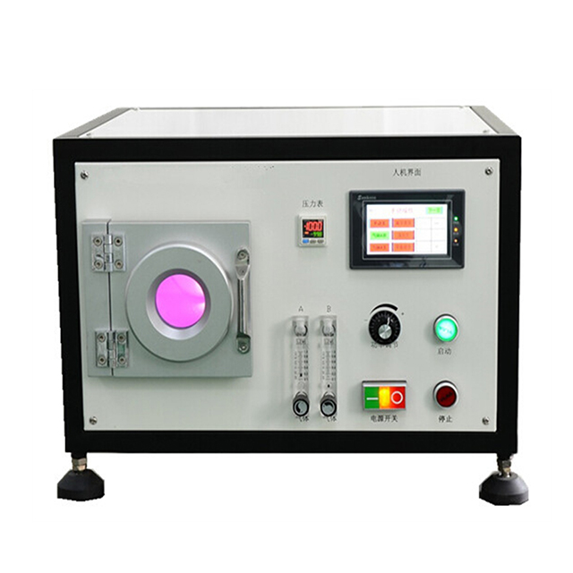
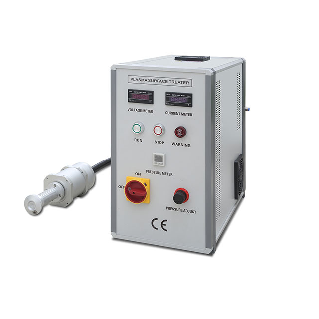
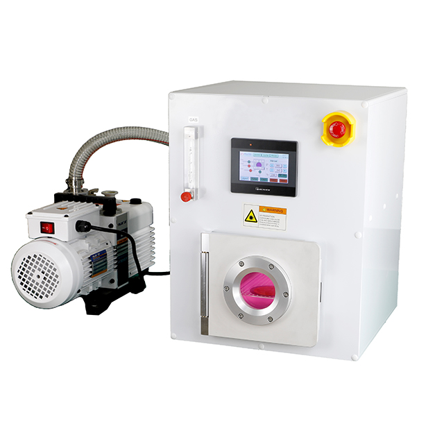
KS-PL-2S vacuum plasma cleaning machine uses energy conversion technology to convert gas into highly active gas plasma with electric energy under a certain vacuum negative pressure. Gas plasma can gently wash the surface of solid sample and cause molecular structure. The change is to achieve ultra-cleaning of organic pollutants on the surface of the sample. In a very short time, the organic pollutants are completely removed by the external vacuum pump, and the cleaning ability can reach the molecular level. Under certain conditions, the surface characteristics of the sample can also be changed. Since the gas is used as the medium for the cleaning treatment, the re-contamination of the sample can be effectively avoided. Plasma cleaners enhance sample adhesion, compatibility and wetting, as well as disinfect and sterilize samples. Plasma cleaning machines are now widely used in the fields of optics, optoelectronics, electronics, materials science, polymers, biomedicine, microfluidics, etc.
Advantages
It has the characteristics of stable performance, high cost performance, easy operation, low cost of use and easy maintenance.
Ultra-cleaning and modification of surfaces of metals, ceramics, glass, silicon wafers, plastics, etc. with various geometric shapes and surface roughness.
Thoroughly remove organic contaminants from the sample surface.
Timed processing, fast processing, and high cleaning efficiency.
It is environmentally friendly, does not use chemical solvents, and has no secondary pollution to samples and the environment.
Ultra-cleaning is carried out under normal temperature conditions, and the sample is non-destructively treated.
Application Field
Ultra-cleaning of optical components, electronic components, semiconductor components, laser devices, coated substrates, terminal mounting, and the like.
Cleaning a variety of lenses and slides such as optical lenses and electron microscopes.
The photoresist material on the surface of the optical element, the semiconductor element, or the like is removed to remove the oxide on the surface of the metal material.
Cleaning semiconductor components, printed wiring boards, ATR components, intraocular lenses, natural crystals and gemstones.
Technical Parameters
| Stainless steel chamber | Φ100mm × 270mm |
| Capacity | 2 liters |
| Power supply | AC220V |
| Working current | not more than 1.2A (excluding vacuum pump) |
| RF power supply | 0-150W/0-300W (select a section before leaving the factory) |
| RF frequency | 40KHz or 13.56MHz optional (offset less than 0.2KHz) |
| Frequency offset | less than 0.2KHz |
| Characteristic impedance | 50 ohms, automatic matching |
| Vacuum degree | 10Pa-1000Pa |
| Gas flow | 60-600ml/min (adjustable) |
| Process control | MCU automatic and manual mode |
| Cleaning time | 1-100 minutes adjustable |
| Power size | 10%-100% adjustable |
| Dimensions | 400x450x250 |
| Weight | 36.5Kg |
| Vacuum pump | 2XZ-4 |
| Vacuum chamber temperature | less than 65 ° C |
| Cooling method | Forced air cooling |


